
量子效率测试仪
PL/EL一体机
Sinton硅片少子寿命测试仪
Sinton硅块少子寿命测试仪
绒面反射率测试仪
3D共聚焦显微镜
在线SiN膜厚测试仪
在线反射率测试仪
在线四探针方阻测试仪
全自动扫描四探针方阻测试仪
在线薄膜厚度测试仪
晶化率测试仪
Horiba显微共焦拉曼光谱仪
傅里叶红外光谱仪
霍尔效应测试仪
分光光度计
全光谱椭偏仪
Horiba椭圆偏振光谱仪
TLM接触电阻率测试仪
超景深显微镜
网版智能影像测量仪
全自动影像测量仪
卧式拉力机
电池片稳态光衰老化试验箱
电池片紫外老化试验箱
电池片拉脱力综合测试仪
外观检验台
湿漏电测试系统
组件实验室EL测试仪
紫外老化试验箱
稳态光衰老化试验箱
电流连续性监测系统
PID测试系统
旁路二极管测试系统
LeTID测试系统
反向电流过载系统
脉冲电压测试系统
绝缘耐压测试仪
接地连续性测试仪
绝缘耐压接地测试仪
湿热环境试验箱
湿冻环境试验箱
热循环试验箱
动态机械载荷测试机
静态机械载荷测试机
冰雹冲击试验机
引出端强度试验机
霰弹冲击试验机
抗划伤(切割)测试机
剥离试验机
万能材料试验机(单臂)
万能材料试验机(双臂)
光伏玻璃透过率测试仪
醋酸测试试验箱
交联度测试系统
二极管接线盒综合测试仪
落球冲击试验机
半自动四探针
全自动探针式台阶仪
多通道太阳能MPPT系统
Horiba稳瞬态荧光光谱仪
大面积钙钛矿方阻椭偏二合一测试仪
大面积钙钛矿影像显微二合一监测站
钙钛矿P1激光划线测试仪
钙钛矿在线PL测试仪
钙钛矿在线方阻测试仪
钙钛矿在线膜厚测试仪
钙钛矿工艺检测工作站
便携式EL测试仪
手持热成像测试仪
户外组件多通道测试系统
光伏逆变器电能质量测试仪
无人机EL检测仪
光热真空老化试验箱
IV测试仪
IVEL分选机
动态机械载荷测试前后光伏组件的效率对比
日期:2024-08-13浏览量:1005
光伏(PV)模块在现场的使用寿命预计至少为20年。为了确保这一点,光伏组件的机械完整性非常重要,影响光伏模块效率的关键因素之一是其安装环境的外部气候条件的多样性。「美能光伏」动态机械载荷测试仪通过模拟环境不同的动态和静态机械载荷,测试光伏模块性能和影响,有助于提高光伏模块的可靠性和使用寿命。
机械负载测试是为了测试光伏模块在2400 Pa和5400 Pa均匀负载下的可靠性。根据IEC-61215标准,在光伏模块表面施加载荷3小时,在负载前后进行电致发光(EL)成像和太阳辐照测试,以表征负载对PV的性能和影响。
验证与测试
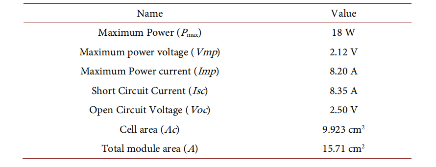
根据电池的类型(单晶和多晶)和母线的数量(3和4)对PV进行了区分和命名:单晶3母线(MT-3BB)、单晶4母线(MT-4BB)、多晶3母线(PT-3BB)和 多晶4母线(PT-4BB)。PV的重要额定规格如表所示:
压力(约5400 Pa)在不同母线数量和电池类型的PV前表面使用测试装置施加3小时。IEC标准,该压力等于PV整个使用寿命期间的模拟机械载荷。为了得到负载的平均效应,按照下图所示的方案,对每种型号的3个PV进行测试。
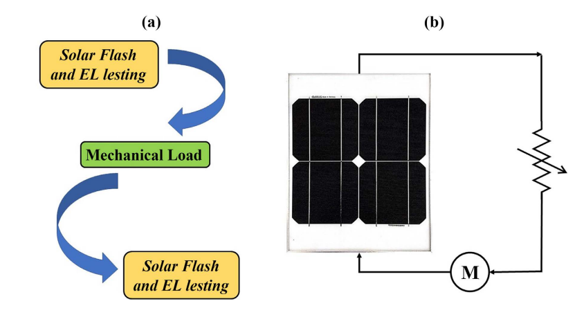
(a) 光伏组件机械测试所用的方法(b)光伏组件的太阳闪光试验设计的电路图
对具有不同母线数量的单晶和多晶串联PV进行了测试,同步对比PV的机械完整性和电性能参数,如功率、效率、填充系数、 串联电阻等,并对施加负载前后的性能进行了比较。重要的电性能参数是通过太阳辐照测试确定的。使用下式计算施加负载前后的最大功率输出:
其中,“I”为PV输出的最大电流,“V”为太阳辐照测试时产生的最大电压。同理,PV的效率由下式确定:
式中“P”为给定太阳辐照度水平“E”时PV的最大功率输出。 式中“A”为组件的总面积。在PV的整体性能中,另一个重要的电气参数是填充系数。填充因子由下式计算:
这里的“Voc”是开路电压,“Isc”是通过太阳辐照测试确定的短路电流。提供给电流流动的电阻也是PV可靠性的一个重要参数(PV串联电阻)由下式确定:

机械载荷负载前后PV的效率变化趋势
对于所有类型的PV,效率仍然大于15%。PT- 4BB模块的效率最小降低了9%,而MT-3BB模块的效率最大降低了20%。
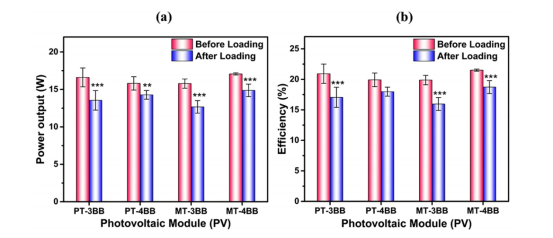
不同类型光伏组件负载前后的功率和效率
不同类型PV的整体性能,填充系数和串联电阻分别如图所示。MT-4BB的填充系数最高,为82%±0. 65%,加载后填充系数为71%±4.03%。MT-3BB的填充系数最低,加载后后是60%±3.99%。
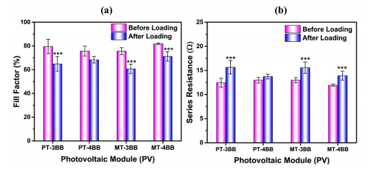
(a)填充系数 (b)负载前后不同型号光伏组件的串联电阻
组件的功率输出和效率由多种参数决定,包括接收的辐照量、使用的玻璃的反射率、制造的制造工艺以及组件的机械完整性。机械载荷对PT-3BB、MT-3BB和MT-4BB电性能的显著影响(p < 0.05)。然而,在PT-4BB模块的情况下,效果不太显著,这背后的原因在于太阳能电池的制造工艺不同。
综上所述,在生产流程的中引入并优化机械载荷模拟测试步骤。模拟组件可能遇到的各种极端环境载荷,如强风、积雪、覆冰等,确保组件在设计、生产阶段就能充分验证其在实际应用中的性能表现。不仅能提升产品的整体质量,还能增强产品的市场竞争力,为用户提供更加可靠、耐用的太阳能光伏组件。
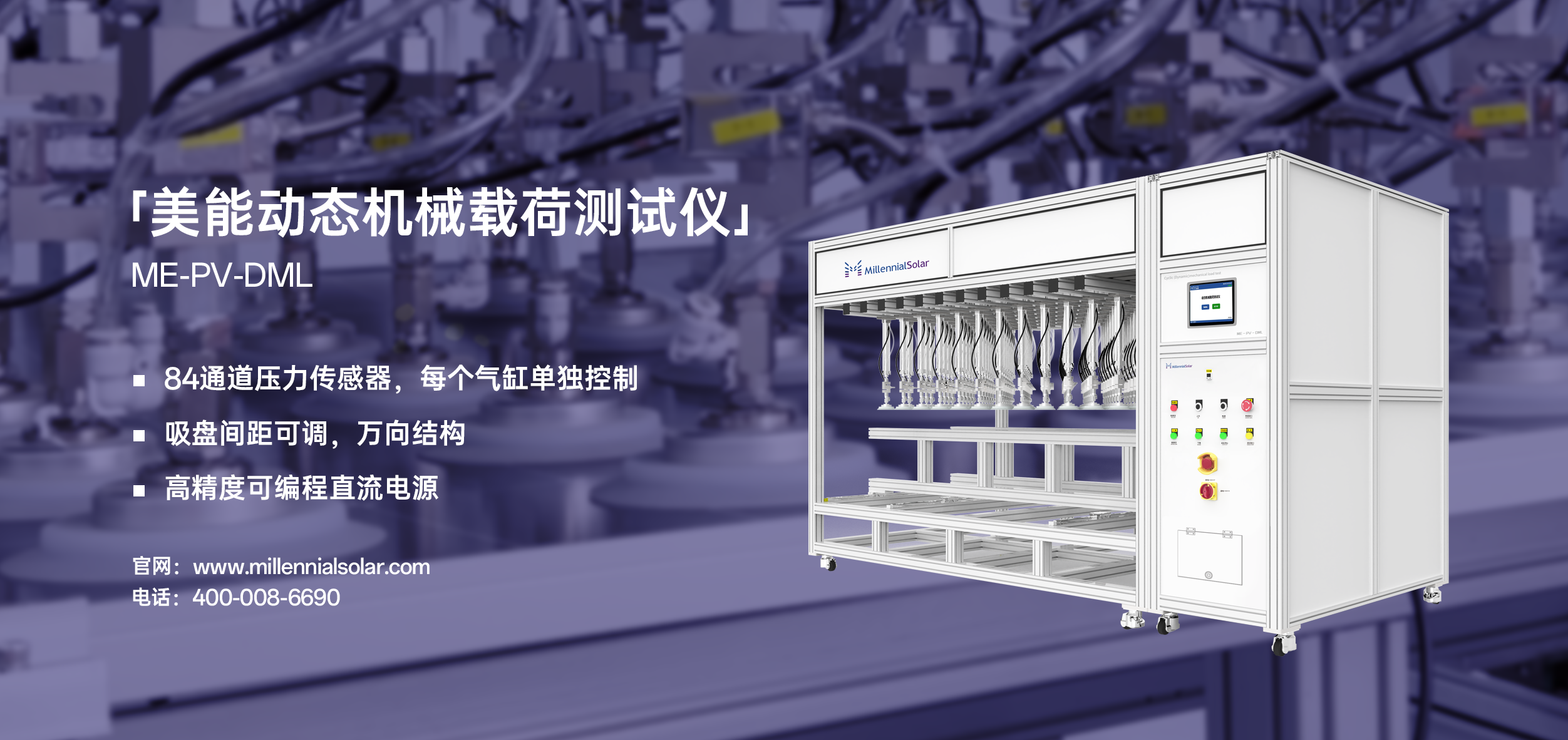
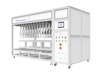
美能动态机械载荷测试仪
联系电话:400 008 6690
「美能动态机械载荷测试仪」ME-PV-DML 84通道压力传感器控制,每个气缸单独控制;吸盘间距可调,万向结构,保障组件表面受力均匀,高精度可编程直流电源监控组件内部电流连续性。
载荷施加方式:气缸带动吸盘压合吸;
可安装多达84(12*7)个气缸,每个气缸单独控制;
测试系统压力,拉力,保持时间,循环测试,循环频率,电流大小可以预先设定;
测试系统可记录和存储测试过程中的正向压强,反向压强,形变,温度,循环次数,电流值。
通过模拟环境不同的机械载荷,测试光伏模块性能和影响,有助于提高光伏模块的可靠性和使用寿命。「美能光伏」动态机械载荷测试仪,兼具静态载荷和动态载荷测试功能,模拟组件承受正反方向交替加压试验,加速组件材料疲劳,检验组件的真实可靠性。
market@millennialsolar.com
江苏省苏州市吴中区金地威新吴中智造园21栋


扫一扫
关注技术顾问
扫一扫
关注官方公众号
扫一扫
关注官方视频号
扫一扫
关注B站视频号
提供以下信息与我们联系,我们很乐意为您提供帮助!
江苏美能测试集团有限公司 版权所有 © 2022 苏ICP备2020061695号-7


