
量子效率测试仪
PL/EL一体机
Sinton硅片少子寿命测试仪
Sinton硅块少子寿命测试仪
绒面反射率测试仪
3D共聚焦显微镜
在线SiN膜厚测试仪
在线反射率测试仪
在线四探针方阻测试仪
全自动扫描四探针方阻测试仪
在线薄膜厚度测试仪
晶化率测试仪
Horiba显微共焦拉曼光谱仪
傅里叶红外光谱仪
霍尔效应测试仪
分光光度计
全光谱椭偏仪
Horiba椭圆偏振光谱仪
TLM接触电阻率测试仪
超景深显微镜
网版智能影像测量仪
全自动影像测量仪
卧式拉力机
电池片稳态光衰老化试验箱
电池片紫外老化试验箱
电池片拉脱力综合测试仪
外观检验台
湿漏电测试系统
组件实验室EL测试仪
紫外老化试验箱
稳态光衰老化试验箱
电流连续性监测系统
PID测试系统
旁路二极管测试系统
LeTID测试系统
反向电流过载系统
脉冲电压测试系统
绝缘耐压测试仪
接地连续性测试仪
绝缘耐压接地测试仪
湿热环境试验箱
湿冻环境试验箱
热循环试验箱
动态机械载荷测试机
静态机械载荷测试机
冰雹冲击试验机
引出端强度试验机
霰弹冲击试验机
抗划伤(切割)测试机
剥离试验机
万能材料试验机(单臂)
万能材料试验机(双臂)
光伏玻璃透过率测试仪
醋酸测试试验箱
交联度测试系统
二极管接线盒综合测试仪
落球冲击试验机
半自动四探针
全自动探针式台阶仪
多通道太阳能MPPT系统
Horiba稳瞬态荧光光谱仪
大面积钙钛矿方阻椭偏二合一测试仪
大面积钙钛矿影像显微二合一监测站
钙钛矿P1激光划线测试仪
钙钛矿在线PL测试仪
钙钛矿在线方阻测试仪
钙钛矿在线膜厚测试仪
钙钛矿工艺检测工作站
便携式EL测试仪
手持热成像测试仪
户外组件多通道测试系统
光伏逆变器电能质量测试仪
无人机EL检测仪
光热真空老化试验箱
IV测试仪
IVEL分选机
紫外线诱导降解(UVID)对TOPCon光伏组件的影响
日期:2024-09-27浏览量:3500
TOPCon光伏组件随着技术的成熟和成本的降低,在全球范围内得到了迅速的推广和应用。然而,由于电池对紫外线辐射的敏感性增加,TOPCon技术容易受到紫外线诱导降解(UVID)的影响,这对组件的性能、寿命和保修均产生了影响。美能紫外老化试验箱,可通过模拟不同光照情况来监控组件在光照下产生的变化,可用于光伏组件产品开发和质量把控或评估组件组成后耐用性的变化试验。
可再生能源测试中心(RETC)于2024年发布的组件报告中指出,n-TOPCon电池组件中UVID(紫外线诱导衰减)风险呈上升态势。RETC表示,部分新型电池技术(其中最为明显的当属 n-TOPCon)似乎较为容易受到UVID的影响。在测试的模型中,有40%达到了UVID高标准,这意味着衰减率低于2%。由此可见,UVID极有可能成为目前面临的主要可靠性问题。
UVID诱导降解模式
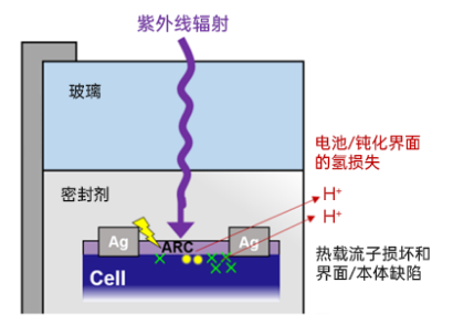
UVID诱导降解模式
SiNx/Si界面的复合:UV 光子能量>3.5eV(λ<360nm)时,会打破SiNx/Si界面的Si - H键。通过产生悬挂键,降低了钝化质量,从而增加了发射极饱和电流并降低了载流子寿命。
硅体复合:UV会导致载流子注入,改变杂质电荷状态(和迁移率),并且在转移过程中结合形成体缺陷中心。这种体缺陷中心的形成会进一步影响电池的性能和稳定性。
热载流子效应:产生热电子(具有高迁移率和高动能),当热电子超过界面势垒时,会损坏钝化层并增加界面态密度。这一效应也对电池的钝化层等关键结构造成破坏,进而影响电池的整体性能。
UVID 测试过程及条件
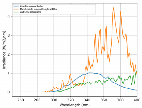
在60°C 短路条件下,组件正面暴露于120kWh/m²的 UV(280 - 400nm)。总UV剂量相当于 1 - 2 年的户外暴露量(具体取决于位置)。UVID 测试设置符合 IEC61215:2021 MQT10 要求,使用金属卤化物灯,UVB含量在3-9% 范围内。
功率降解情况分析
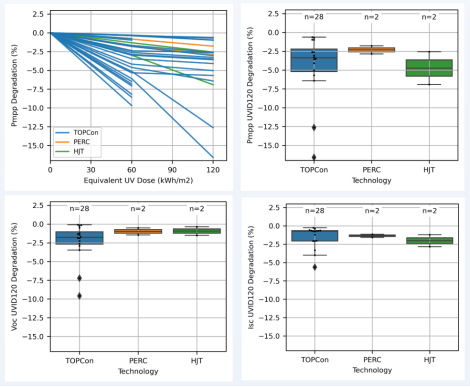
整体功率损失范围:
UVID - 120 后功率损失从0.6%到16.6% 不等。这一数据显示出不同组件在 UVID 测试后的功率损失差异较大,反映了组件对 UVID 的敏感性存在差异以及不同组件的抗降解能力不同。
TOPCon 组件的功率降解情况:
超过 50% 的 TOPCon 组件呈现出功率降解>5%/年,这表明 TOPCon组件在 UVID 影响下功率降解较为明显,是需要重点关注和研究解决的问题。
受影响参数分析:
Voc是受影响最大的参数,归因于钝化损失;其次是 Isc 和 FF。在性能良好的组件中,Isc 损失最小。这种参数受影响的差异为深入研究 UVID 降解机制和改进组件性能提供了重要的线索和方向。
应对 UVID 的措施及进展
紫外线会影响 TOPCon 电池钝化层,光伏制造商正在积极寻求处理方法以减轻这种影响。通过遵循 IEC61215:2021 MQT10 对紫外线检测标准和程序,部分制造商似乎已经在一定程度上控制了 UVID。
确保 TOPCon 组件抗 UVID 的最佳方法之一是通过 UV 测试,这有助于筛选出性能优良的组件,提高产品的可靠性和稳定性,以满足市场对高质量光伏组件的需求。
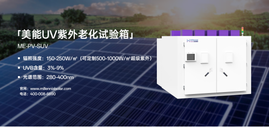
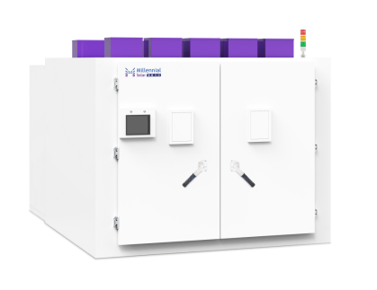
美能UV紫外老化试验箱
联系电话:400 008 6690
美能UV紫外老化试验箱,通过模拟不同光照情况来监控组件在光照下产生的变化,可用于光伏组件产品开发和质量把控或评估组件组成后耐用性的变化试验。
n辐照强度:150-250W/㎡(可定制500-1000W/㎡超级紫外)
nUVB含量:3%-9%
n光谱范围:280-400nm
通过紫外线(UV)老化测试,为整个光伏行业在应对 UVID 问题上提供了有益的经验和借鉴,推动行业不断改进技术和提高产品质量。美能UV紫外老化试验箱,能够详细评估组件在长期环境暴露后的稳定性,还能为产品开发和质量控制提供关键数据。
market@millennialsolar.com
江苏省苏州市吴中区金地威新吴中智造园21栋


扫一扫
关注技术顾问
扫一扫
关注官方公众号
扫一扫
关注官方视频号
扫一扫
关注B站视频号
提供以下信息与我们联系,我们很乐意为您提供帮助!
江苏美能测试集团有限公司 版权所有 © 2022 苏ICP备2020061695号-7


